1. High performance, visible to mid-infrared photodetector
1.1 Atomically thin noble metal dicholcogenide: a broadband mid-infrared semiconductor
Graphene has drawn tremendous attention as a promising candidate for electronic and optoelectronic applications owing
to its extraordinary properties, such as broadband absorption and ultrahigh mobility. Nevertheless, the absence of
bandgap makes graphene unfavorable for digital electronic or photonic applications. Although patterning graphene into
nanostructures with quantum confinement effect is able to open a bandgap, devices based on these graphene
nanostructures generally suffer from the low carrier mobility and scattering losses. In this paper, we demonstrated that
encapsulation of atomic layer deposited high-quality HfO2 film will greatly enhance the carrier mobility and decrease the
scattering losses of graphene nanoribbon, because this high-k dielectric layer weakens carrier Coulombic interactions. In
addition, photodetector based on HfO2 layer capped graphene nanoribbons can cover a broadband wavelength from
visible to mid-infrared at room temperature, exhibiting ~10 times higher responsivity than the one without HfO2 layer in
visible regime and ~8 times higher in mid-infrared regime. The method employed here could be potentially used as a
general approach to improve the performance of graphene nanostructures for electronic and optoelectronic applications.
View large figure |
|
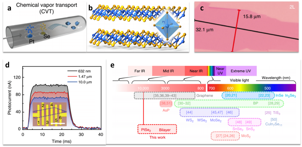
Fig. 1 (a) Illustrative diagram of experimental setup for the growth of PtSe2single crystals by CVT method.
(b) Crystal structure of PtSe2andbits three-dimensional (3D) side views.
(c) Optical microscope images monolayer PtSe2. (d) Optoelectronic properties of the monolayer and the bilayer PtSe2.
(e) Comparison of photodetectors operated at different wavelengths, based on two-dimensional materials, such as graphene,
MoS2, black phosphorene, WS2, WSe2, MoSe2, SnSe2, SnS2, InSe, In2Se3, TiS3, CuIn7Se11, and black AsP. The mid-infrared range is rarely explored besides graphene.
|
| |
|
|
X. Yu, P. Yu, D. Wu, B. Singh, Q. Zeng, H. Lin, W. Zhou, Z. Liu and Q.J. Wang*,
"Atomically thin noble metal dichalcogenide: a broadband mid-infrared semiconductor", Nature Communications 9, 1545, 2018.
TOP
1.2 Narrow bandgap oxide nanoparticles coupled with graphene for high performance mid-infrared photodetection
The pursuit of optoelectronic devices operating in the mid-infrared regime is driven by both
fundamental interests and envisioned applications ranging from imaging, sensing to communications. Despite continued achievements
in traditional semiconductors, notorious obstacles such as the complicated growth processes and cryogenic operation preclude the usage
of infrared detectors. As an alternative path towards high-performance photodetectors, hybrid semiconductor/graphene structures have
been intensively explored. However, the operation bandwidth of such photodetectors has been limited to visible and near-infrared regimes.
Here we demonstrate a mid-infrared hybrid photodetector enabled by coupling graphene with a narrow bandgap semiconductor, Ti2O3(Eg=0.09 eV),
which achieves a high responsivity of 300 AW−1 in a broadband wavelength range up to 10μm. The obtained responsivity is about two
orders of magnitude higher than that of the commercial mid-infrared photodetectors. Our work opens a route towards achieving high-performance
optoelectronics operating in the mid-infrared regime.
View large figure |
|
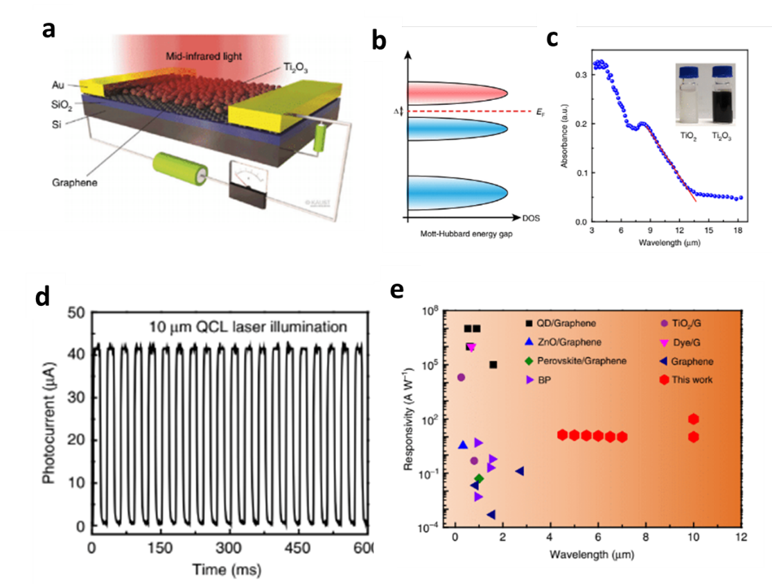
Figure 1. (a) Schematic diagram of hybrid graphene/Ti2O3 nanoparticle photodetector.
(b) chematic band diagram of Ti2O3, indicating that a narrow bandgap is formed between upper Hubbard band (pink) and lower Hubbard band (blue)
as a result of strong electron correlation.
(c) Absorption spectrum of Ti2O3nanoparticles drop-casted on a KBr substrate, measured through Fourier
Transform Infrared Spectroscopy. (d) Temporal response of the device to the illumination of 10μm laser.
(e) Comparison of the performance of the hybrid graphene/Ti2O3photodetector with the state-of-the-art.
|
X. Yu, Y.Li, X. Hu, D. Zhang, Y. Tao, M. Haque, T. Wu, Z. Liu and Q.J. Wang*, "Narrow bandgap oxide
nanoparticles coupled with graphene for high performance mid-infrared photodetection",
Nature Communication 9, 4299, 2018.
TOP
2. Mid-infrared Phonon Polaritons
Highly confined polaritons hold great promises in demonstrating unprecedented classical and quantum phenomena,
such as strong coupling, perfect lensing and highly confined hyperbolic dispersions. It also lays a foundation for building optoelectronic devices
with nanoscale fingerprint and realizing functionalities such as high sensitivity biosensing, super resolution imaging, subdiffractional focusing
and single molecule chemical sensing. The performance of these devices rooted in the polariton properties, such as confinement and material loss.
The phonon polariton exist in polar crystals in longer wavelength (Mid-IR to THz) and exhibit material losses a few orders smaller than the plasmon
polaritons. Some polar crystals have extreme anisotropic optical properties along different crystalline directions which makes them excellent
platform for building hyperbolic devices. In our group, we are interested in the fundamental properties of phonon polaritons, especially in hybrid
heterostructures. We also target to demonstrate phonon polariton based nanodevices such as nanoresonators, metamaterials and sensors. Our studies
pave the ways towards new generation of polariton-based high performance optoelectronic and nanophotonics devices.
View large figure |
|
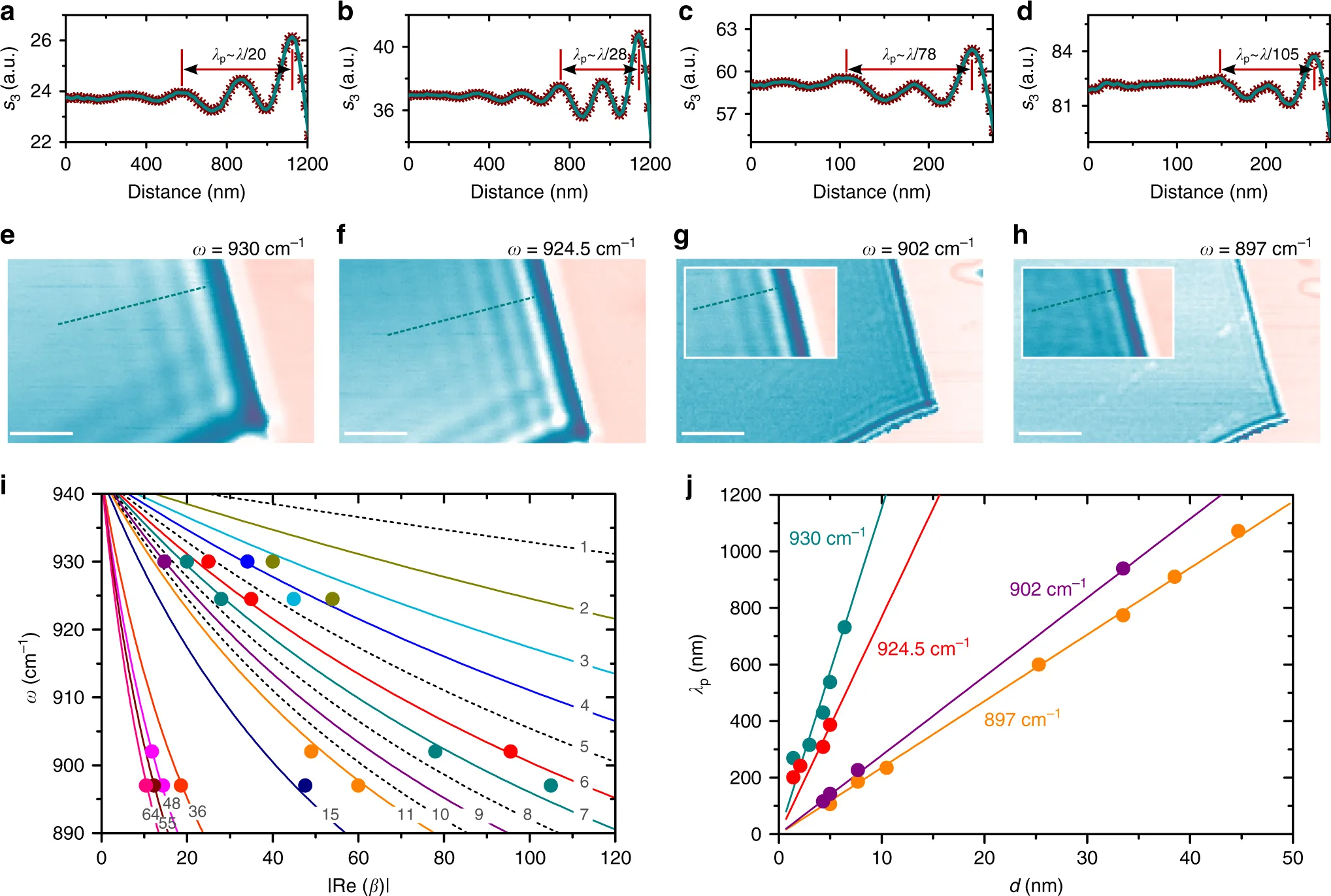
Fig.1 Highly confined phonon polariton states in MoS2–SiC heterostructures.a–hNear-field images
(optical amplitudes3) of 7-layer MoS2on SiC (e–h)recorded at different laser excitation lines (marked asω), and corresponding cross-sections
(a–d) along cyan dotted lines.
Cyan and pink colours refer toMoS2crystal and the substrate (SiC) areas correspondingly.
Cyan curves in images (a–d) serve as eye guide.
Cyan curves in images (a–d) serve as eye guide. Insets in images (g,h) show zoomed infringes on
the top right hand side part of MoS2–SiC boundary. Scale bars are 500 nm.iCalculated (solid/dotted curves) and experimental (circles)
dispersion for different number of MoS2layers (labelled on each of the curves).
Data corresponding to the same number of layers are marked with the same colour.j
Calculated and experimental scaling of the SPhPs wavelength with MoS2thickness. Data corresponding to the same laser line
are marked with the same colour.
|
| |
|
|
View large figure |
|
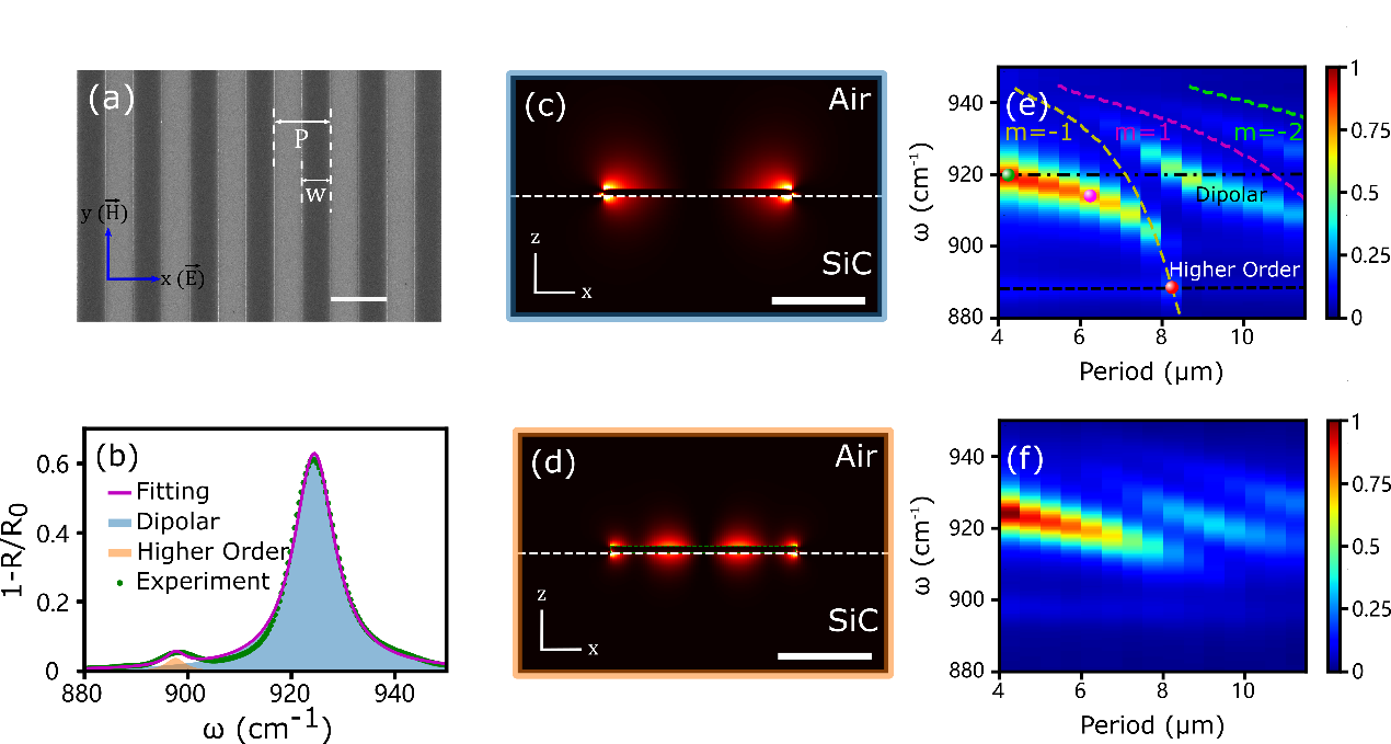
Fig. 2 Localized hybrid phonon resonance of Ge grating on SiC and its coupling with SPhP.
(a) SEM image of the grating (w=2 μm and P=4 μm). Scale bar equals 4μm.
(b) Measured absorption spectrum of gratings in (a) and its double-Lorentzian fittings. Simulated intensity distribution of the
(c) dipolar and (d) higher order mode.
The (e) simulated (f) experimental measured reflection spectra shows that the dipolar mode could
be coupled to the SPhP mode when the periods of the grating meets the phase matching conditions. The dash line in (e) marks the phase
matching condition for different grating orders m.
|
| |
|
|
A. M. Dubrovkin, , B. Qiang, H. N. S. Krishnamoorthy, N. I. Zheludev and Q. J. Wang*, "Ultra-confined surface
phonon polaritons in molecular layers of van der Waals dielectrics",
Nature Communications, 9, 1726, 2018.
B. Qiang, A. M. Dubrovkin, H. N. S. Krishnamoorthy, Q. Wang, C. Soci, Y. Zhang, J. Teng, Q. J. Wang*, "High
Q-factor controllable phononic modes in hybrid phononic dielectrics",
Advance Photonics 1(2), 026001, 2019.
TOP
3. Graphene plasmonics
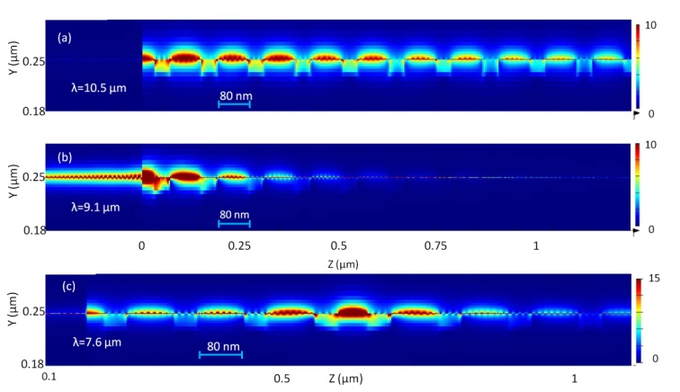
We propose and numerically analyze a plasmonic Bragg reflector formed in graphene waveguide. The results show that the graphene plasmonic Bragg reflector can produce a broadband stopband, which can be tuned over a wide wavelength range by a small change in Fermi energy level of graphene. By introducing a defect into the Bragg reflector, we can achieve a Fabry-Perot-like microcavity with a quality factor of 50 for the defect resonance mode formed in the stopband. The proposed Bragg reflector could be used as a broadband ultrafast tunable integrated filter and a broadband modulator. In addition, the defect microcavity may find applications in graphene based resonators.
View large figure |
|
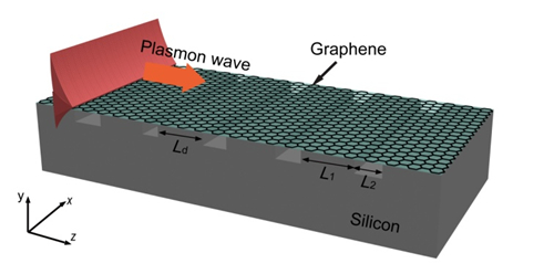
Fig. 1 Schematic of graphene plasmonic Bragg reflector formed in silicon grating substrate. |
| |
|
|
View large figure |
|
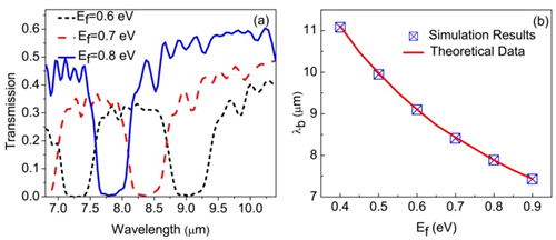
Fig 2 (a) Simulated transmission spectra of graphene plasmonic reflector with different Fermi energy levels when µ = 10000 cm2/ (V·s).
(b) Bragg wavelength as a function of Fermi energy level. The squares are simulated results from FDTD, and the red line is theoretical data. The lengths of the graphene-silicon, graphene-air waveguide are L1 = 80 nm, L2 = 40 nm, respectively. The period of Bragg cell N is 10.
|
| |
|
|
View large figure |
|
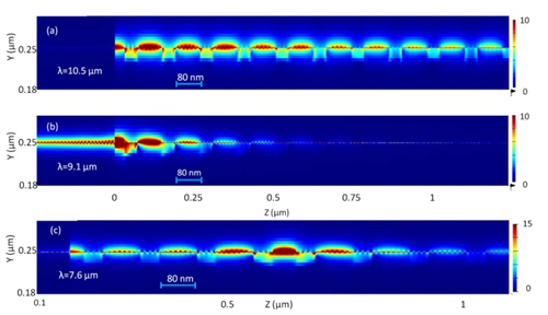
Fig. 3. (a) and (b) Simulated electric field intensity profiles of the plasmonic Bragg reflectors at the incident wavelength at 10.5 µm and 9.1 µm.
(c) Corresponds to the defect resonance mode at 7.6 µm. |
| |
|
|
J. Tao, X. Yu, B. Hu, A. Dubrovkin, and Q. J. Wang*, "Graphene-based tunable plasmonic Bragg reflector with a broad bandwidth", Optics Letters 39, 271-274, 2014.
TOP
|